- 您现在的位置:买卖IC网 > Sheet目录364 > SST25VF010A-33-4I-QAE-T (Microchip Technology)IC FLASH SER 1MB 33MHZ SPI 8WSON
�� �
�
�1� Mbit� SPI� Serial� Flash�
�A� Microchip� Technology� Company�
�SST25VF010A�
�Data� Sheet�
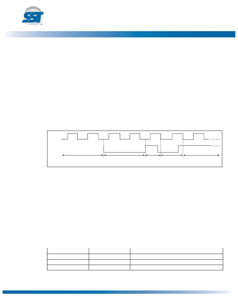
�Hold� Operation�
�HOLD#� pin� is� used� to� pause� a� serial� sequence� underway� with� the� SPI� flash� memory� without� resetting�
�the� clocking� sequence.� To� activate� the� HOLD#� mode,� CE#� must� be� in� active� low� state.� The� HOLD#�
�mode� begins� when� the� SCK� active� low� state� coincides� with� the� falling� edge� of� the� HOLD#� signal.� The�
�HOLD� mode� ends� when� the� HOLD#� signal’s� rising� edge� coincides� with� the� SCK� active� low� state.�
�If� the� falling� edge� of� the� HOLD#� signal� does� not� coincide� with� the� SCK� active� low� state,� then� the� device�
�enters� Hold� mode� when� the� SCK� next� reaches� the� active� low� state.� Similarly,� if� the� rising� edge� of� the�
�HOLD#� signal� does� not� coincide� with� the� SCK� active� low� state,� then� the� device� exits� in� Hold� mode�
�when� the� SCK� next� reaches� the� active� low� state.� See� Figure� 3� for� Hold� Condition� waveform.�
�Once� the� device� enters� Hold� mode,� SO� will� be� in� high-impedance� state� while� SI� and� SCK� can� be� V� IL� or� V� IH� .�
�If� CE#� is� driven� active� high� during� a� Hold� condition,� it� resets� the� internal� logic� of� the� device.� As� long� as�
�HOLD#� signal� is� low,� the� memory� remains� in� the� Hold� condition.� To� resume� communication� with� the�
�device,� HOLD#� must� be� driven� active� high,� and� CE#� must� be� driven� active� low.� See� Figure� 18� for� Hold�
�timing.�
�SCK�
�HOLD#�
�Active�
�Hold�
�Active�
�Hold�
�Active�
�1265� F03.0�
�Figure� 3:� Hold� Condition� Waveform�
�Write� Protection�
�The� SST25VF010A� provides� software� Write� protection.� The� Write� Protect� pin� (WP#)� enables� or� dis-�
�ables� the� lock-down� function� of� the� status� register.� The� Block-Protection� bits� (BP1,� BP0,� and� BPL)� in�
�the� status� register� provide� Write� protection� to� the� memory� array� and� the� status� register.� See� Table� 5� for�
�Block-Protection� description.�
�Write� Protect� Pin� (WP#)�
�The� Write� Protect� (WP#)� pin� enables� the� lock-down� function� of� the� BPL� bit� (bit� 7)� in� the� status� register.�
�When� WP#� is� driven� low,� the� execution� of� the� Write-Status-Register� (WRSR)� instruction� is� determined�
�by� the� value� of� the� BPL� bit� (see� Table� 3).� When� WP#� is� high,� the� lock-down� function� of� the� BPL� bit� is�
�disabled.�
�Table� 3:� Conditions� to� execute� Write-Status-Register� (WRSR)� Instruction�
�WP#�
�L�
�L�
�H�
�BPL�
�1�
�0�
�X�
�Execute� WRSR� Instruction�
�Not� Allowed�
�Allowed�
�Allowed�
�T3.0� 25081�
�?2011� Silicon� Storage� Technology,� Inc.�
�6�
�S725081A�
�10/11�
�发布紧急采购,3分钟左右您将得到回复。
相关PDF资料
SST25VF016B-50-4C-S2AF-T
IC FLASH SER 16M 50MHZ SPI 8SOIC
SST25VF020-20-4C-QAE-T
IC FLASH SER 2MB 20MHZ SPI 8WSON
SST25VF020B-80-4C-QAE-T
IC FLASH SER 2MB 80MHZ SPI 8WSON
SST25VF032B-66-4I-S2AF
IC FLASH SER 32M 66MHZ SPI 8SOIC
SST25VF040B-50-4C-ZAE
IC FLASH SER 4MB 80MHZ SPI 8CSP
SST25VF040B-80-4I-QAE
IC FLASH SER 4MB 80MHZ SPI 8WSON
SST25VF064C-80-4I-Q2AE-T
IC FLASH SER 64M DUAL I/O 8WSON
SST25VF080B-80-4I-QAE-T
IC FLASH SER 8MB 50MHZ SPI 8WSON
相关代理商/技术参数
SST25VF010A-33-4I-SAE
功能描述:闪存 1M (128K x 8) 33MHz RoHS:否 制造商:ON Semiconductor 数据总线宽度:1 bit 存储类型:Flash 存储容量:2 MB 结构:256 K x 8 定时类型: 接口类型:SPI 访问时间: 电源电压-最大:3.6 V 电源电压-最小:2.3 V 最大工作电流:15 mA 工作温度:- 40 C to + 85 C 安装风格:SMD/SMT 封装 / 箱体: 封装:Reel
SST25VF010A-33-4I-SAE
制造商:Microchip Technology Inc 功能描述:MEMORY FLASH 1M SPI 8SOIC
SST25VF010A-33-4I-SAE_
制造商:Microchip Technology Inc 功能描述:
SST25VF010A-33-4I-SAE-T
功能描述:闪存 1M (128Kx8) 33MHz 2.7-3.6V Industrial RoHS:否 制造商:ON Semiconductor 数据总线宽度:1 bit 存储类型:Flash 存储容量:2 MB 结构:256 K x 8 定时类型: 接口类型:SPI 访问时间: 电源电压-最大:3.6 V 电源电压-最小:2.3 V 最大工作电流:15 mA 工作温度:- 40 C to + 85 C 安装风格:SMD/SMT 封装 / 箱体: 封装:Reel
SST25VF010A-33-4I-ZAE
功能描述:闪存 2.7V to 3.6V 1Mbit SPI Serial 闪存 RoHS:否 制造商:ON Semiconductor 数据总线宽度:1 bit 存储类型:Flash 存储容量:2 MB 结构:256 K x 8 定时类型: 接口类型:SPI 访问时间: 电源电压-最大:3.6 V 电源电压-最小:2.3 V 最大工作电流:15 mA 工作温度:- 40 C to + 85 C 安装风格:SMD/SMT 封装 / 箱体: 封装:Reel
SST25VF016B
制造商:SST 制造商全称:Silicon Storage Technology, Inc 功能描述:16 Mbit SPI Serial Flash
SST25VF016B_10
制造商:SST 制造商全称:Silicon Storage Technology, Inc 功能描述:16 Mbit SPI Serial Flash
SST25VF016B_11
制造商:SST 制造商全称:Silicon Storage Technology, Inc 功能描述:16 Mbit SPI Serial Flash